

When Ondrej Krivanek first considered building a device to boost the resolution of electron microscopes, he asked about funding from the U.S. Department of Energy. “The response was not positive,” he says, laughing. He heard through the grapevine that the administrator who held the purse strings declared that the project would be funded “over his dead body.”
“People just felt it was too complicated, and that nobody would ever make it work,” says Krivanek. But he tried anyway. After all, he says, “If everyone expects you to fail, you can only exceed expectations.”
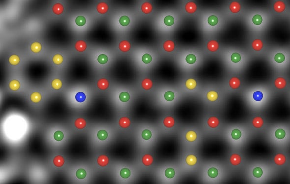
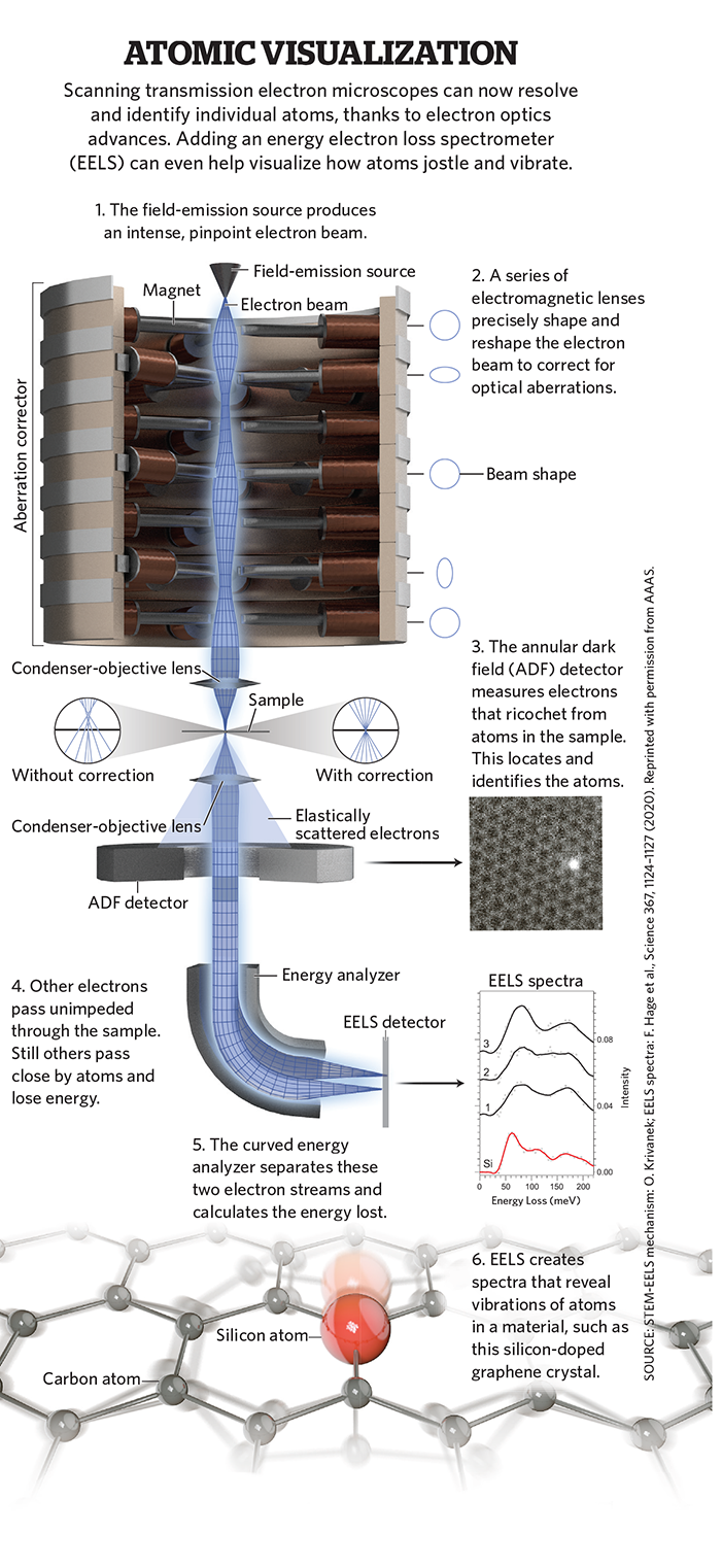
The correctors that Krivanek, Niklas Dellby, and other colleagues subsequently designed for the scanning transmission electron microscope did exceed expectations. They focus the microscope’s electron beam, which scans back and forth across the sample like a spotlight, and make it possible to distinguish individual atoms and to conduct chemical analysis within a sample. For his pioneering efforts, Krivanek shared The Kavli Prize in nanoscience with the German scientists Harald Rose, Maximilian Haider, and Knut Urban, who independently developed correctors for conventional transmission electron microscopes, in which a broad stationary beam illuminates the entire sample at once.
Electron microscopes, invented in 1931, long promised unprecedented clarity, and in theory could resolve objects a hundredth the size of an atom. But in practice they rarely get close because the electromagnetic lenses they use to focus electrons deflected them in ways that distorted and blurred the resulting images.
The aberration correctors designed by both Krivanek’s team and the German scientists deploy a series of electromagnetic fields, applied in multiple planes and different directions, to redirect and focus wayward electrons. “Modern correctors contain more than 100 optical elements and have software that automatically quantifies and fixes 25 different types of aberrations,” says Krivanek, who co-founded a company called Nion to develop and commercialize the technology.
That level of fine-tuning allows microscopists to fix their sights on some important pursuits, such as producing smaller and more energy-efficient computers, analyzing biological samples without incinerating them, and being able to detect hydrogen, the lightest element and a potential clean-burning fuel.
.jpg) Can electron microscopes help build energy-sipping computers?
Can electron microscopes help build energy-sipping computers?
We are making all kinds of fun atomic-scale devices that would minimize the energy needed for a logic operation. Computing on a much lower power budget is a frontier that people are exploring: How many gigaflops can you get per microwatt? What we’re waiting for is a 10-atom transistor built out of foreign atoms incorporated in boron nitride. I’m sure that’s going to come one of these days, because you can move atoms around with the electron beam in these two-dimensional materials. Then the only problem will be trying to connect it to other transistors in the device.
Could microscopy lead to eco-friendly power sources, like hydrogen or solar cells?
Hydrogen fuel cells would be wonderful. It’s one of the most abundant elements, and when you combine hydrogen with oxygen in the air, there’s no pollution because what you’re producing is water. If you could store hydrogen in a storage tank without having to keep it under huge pressure, you could put enough of it in your car. But to put hydrogen into the storage cell and cycle it in and out, you need to be able to see what the hydrogen is doing, where it is sitting, what it is bonded to. That is the province of electron microscopes and their spectrometers, which tell you which elements are where. For solar cells, the issue tends to be efficiency and cost. With silicon solar cells, you get something like 20% efficiency, and you have to grow and slice and polish the silicon crystals, so it can get expensive. Can you make something cheaper and with higher efficiency? What if you could just spray a material as a thin film on a piece of plastic and get good efficiency? When you try to do that, you introduce defects called grain boundaries, because you don’t have a single crystal. There was some nice work from the SuperSEM Laboratory in the U.K. showing how grain boundaries in thin-film solar cells affect their efficiency, and what you can do about it. Microscopy helps us see how we can arrange the internal structure of the material so it gives us the properties we want from an electrical point of view.
How can enhanced resolution advance the study of biological materials?
When you look at an individual cell, you want to understand what type of chemical substances sit at different places, and how they travel in the cell. How are they synthesized, and how are they metabolized into something different? I’m hoping that aberration-corrected vibrational spectroscopy will be able to answer these types of questions. Biological microscopy has typically been a race between extracting useful information from the sample and destroying it with the same beam that you’re using for imaging. In vibrational spectroscopy, you don’t aim the electron beam to the place you’re examining, you direct it nearby. This avoids radiation damage, and allows closer examination of the samples. We can now do this in scanning transmission electron microscopes with remarkable energy and spatial resolution. I was doing a sabbatical at Humboldt University in Berlin, concentrating on precisely this, but I had to finish it prematurely because the university was shutting down due to COVID-19. Hopefully, when the world returns to normal, I’ll go back to Germany, and I’ll be able to say this project worked out great—or, it was a crazy idea and didn’t work at all. If you know how it's going to turn out, then it's engineering. If you don't have any idea, then it's called research. And that's what we're doing right now.
To learn more about brilliant work of Kavli Prize Laureates, visit The Kavli Prize. To explore more of the biggest questions in science, click here.